Search Colleges, Exams, Schools & more


Login
To Study The Characteristics Of A Common Emitter Non (or PNP) Transistor And To Find Out The Values Of Current And Voltage Gains. - Practice Questions & MCQ
Edited By admin | Updated on Sep 18, 2023 18:34 AM | #JEE Main
Quick Facts
-

6 Questions around this concept.
Solve by difficulty
 MEDIUM
Why a common emitter transistor is preferred over a common base transistor?
In a transistor, the current amplification factor is 0.6. a transistor is connected in the same emitter configuration, the change in collector current is when the base current changes by 6mA.
For the transistor, the value of α is 0.8. The change in the collector current corresponding to a change of 4mA in the base current in a common base arrangement is:
JEE Main 2026 Session 2: Result Link | Final Answer Key
JEE Main 2026: College Predictor | Official Question Papers
Comprehensive Guide: IIT's | NIT's | IIIT's | Foreign Universities in India
Don't Miss: India's Best B.Tech Counsellors in your city - Book Your Seat
What is the current gain in common emitter configuration if a change in base current by $10 \mu A$ and collector current increases by 2 MA?
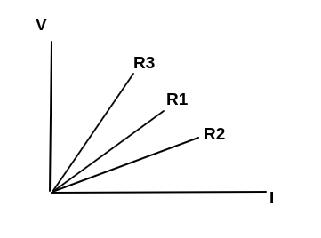
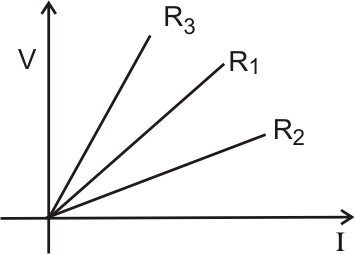
Three resistors of unknown values are measured by measuring current through it and voltage across it. A student plot graph between current and voltage as following. Then
Concepts Covered - 1
To study the characteristics of a common emitter npn (or pnp) transistor and to find out the values of current and voltage gains.
Aim:-
To study the characteristics of a common emitter npn (or pnp) transistor and to find out the values of
current and voltage gains.
Apparatus:-
An n-p-n transistor, a three volt battery, a 30 volt battery, two high resistance rheostats, one 0-3 volt voltmeter, one 0-30 volt voltmeter, one 0-50 micro-ammmeter, one 0 - 50 mA milli-ammeter, two one way keys, connecting wires.
Theory:-
In common-emitter circuit of a transistor, emitter-base make input section and emitter-collector make
output section. As usual, base junction (input junction) is forward biased and collector junction (output
junction) is reverse biased.
Resistance offered by base junction, is called input resistance (R) It has a very small resistance due to forward biasing.
Resistance offered by collector junction, is called output resistance (R0) . \text { It has a high value due to reverse } biasing.
Due to high output resistance (resistance in output section), a high resistance can be used as load resistance ( $R_{\mathrm{L}}$ ). Generally $R_L=R_0$.
The ratio $\frac{R_L}{R_I}=\frac{R_0}{R_I}$ measures resistance gain of the common emitter transistor. It is of the order of one thousand. The current equation, $I_e=I_b+I_c$
Also emitter current ( le ) divides itself into base current $\left(I_b\right)$ and collector current $\left(I_c\right)$. In n-p-n transistor, $I_c$ is about $98 \%$ of $I_e$, base current $I_b$ remains only $2 \%$ of $l_{\mathrm{e}}$. A little change in $l_{\mathrm{b}}$ causes a large change (about 49 times) in $l_{\mathrm{c}}$. The ratio of change in collector current to the corresponding change in base current, measures current gain in common emitter transistor. It is represented by symbol $\beta$.
$
\beta=\frac{\Delta I_c}{\Delta I_b}
$
Formula used:-
Input resistance,
$
R_I=\frac{\Delta V_b}{\Delta I_b}
$
Output resistance,
$
R_o=\frac{\Delta V_c}{\Delta I_c}
$
Resistance gain $=\frac{R_0}{R_I}$
Current gain,
$
\beta=\frac{\Delta I_c}{\Delta I_b}
$
Voltage gain $=$ Current gain $\times$ Resistance gain
$
A_V=\beta \cdot \frac{R_0}{R_I}
$
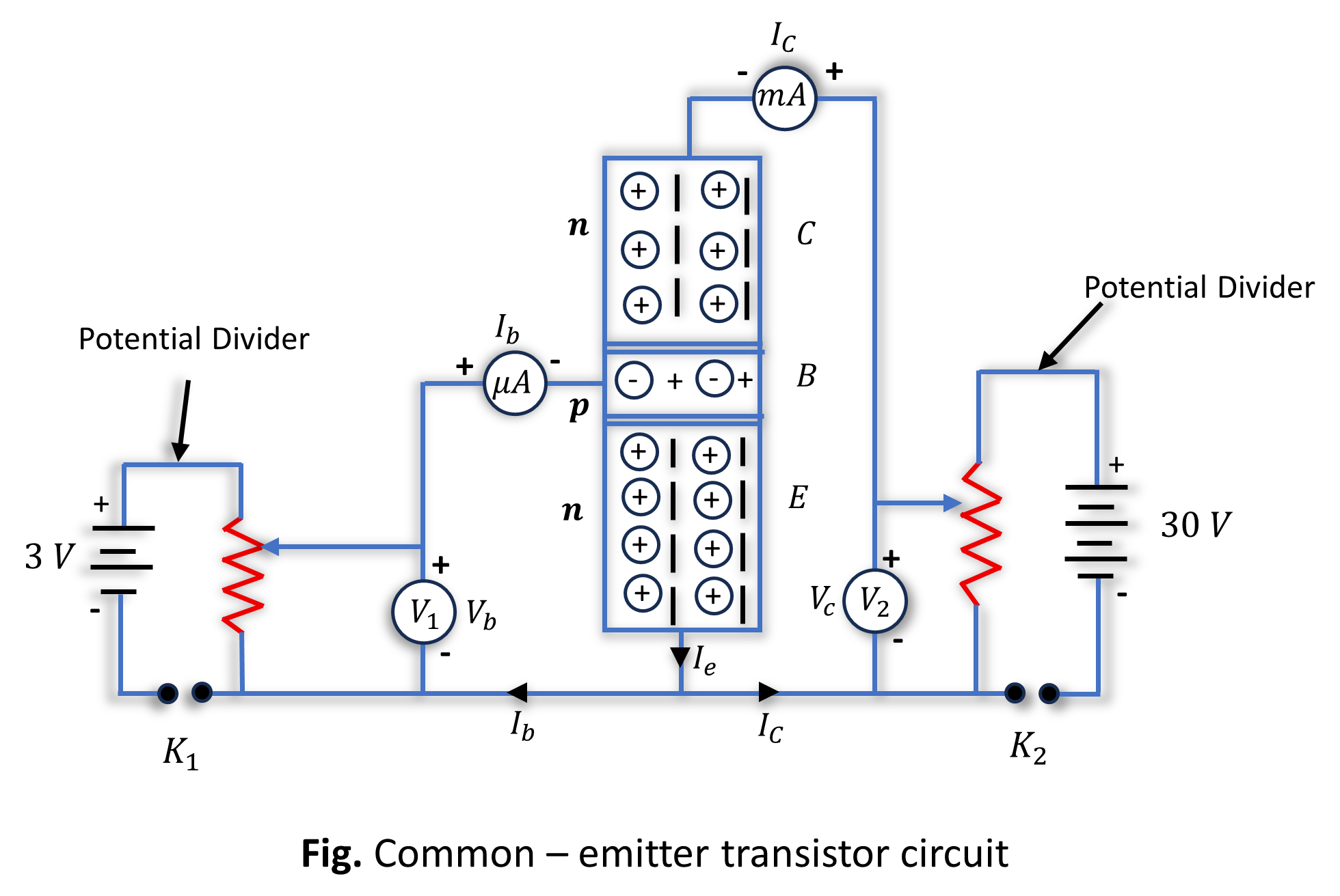
Diagram:-
![]()
Procedure:-
1. Make circuit diagram as shown in figure.
2. Make all connections neat, clean and tight.
3. Note least count and zero errors of voltmeters and ammeters.
4. Make voltmeter readings zero in V1 and V2 and insert the keys.
For input characteristics
5. Apply forward bias voltage on base junction. Read base voltage Vb and base current Ib.
6. Go on increasing $\mathrm{V}_{\mathrm{b} \text { till }} \mathrm{l}_{\mathrm{b}}$ rises suddenly. Note corresponding values of $\mathrm{l}_{\mathrm{b}}$ for each value of $\mathrm{V}_{\mathrm{b}}$.
7. Make collector voltage $\mathrm{V}_{\mathrm{C}}=10 \mathrm{~V}$ and repeat steps 5 and 6 .
8. Repeat step 7 with $\mathrm{V}_{\mathrm{C}}=20 \mathrm{~V}$ and 30 V .
9. Make all readings zero.
For output characteristics
10. Keep collector voltage $\left(\mathrm{V}_{\mathrm{c}}\right)$ zero. Adjust base voltage $\mathrm{V}_{\mathrm{b}}$ to make base current $\mathrm{l}_{\mathrm{b}}=10 \mu \mathrm{~A}$. Though collector voltage $\mathrm{V}_{\mathrm{c}}$ is zero; but there is collector current I ${ }_c$ \{Note it. \}
11. Make collector voltage $10 \mathrm{~V}, 20 \mathrm{~V}$ and 30 V and note the corresponding collector currents.
12. Repeat steps 10 and 11 with $\mathrm{l}_{\mathrm{b}}=20 \mu \mathrm{~A}, 30 \mu \mathrm{~A}$, and $40 \mu \mathrm{~A}$.
13. Record your observations as given below:
Observations:-
Least count of voltmeter, $\quad \mathrm{V}_1=\ldots . . \mathrm{V}$
Zero error of voltmeter, $\quad V_1=\ldots . . \mathrm{V}$
Least count of voltmeter, $\quad \mathrm{V}_2=\ldots . . \mathrm{V}$
Zero error of voltmeter, $\quad \mathrm{V}_2=\ldots . \mathrm{V}$
Least count of milli-ammeter $=\ldots . . \mathrm{mA}$
Zero error of milli-ammeter $\quad=\ldots \mathrm{mA}$
Least count of micro-ammeter $=\ldots \ldots \mu \mathrm{A}$
Zero error of micro-ammeter $\quad=\ldots \ldots . \mu \mathrm{A}$
Calculations:-
1. Calculation for input resistance (RI)
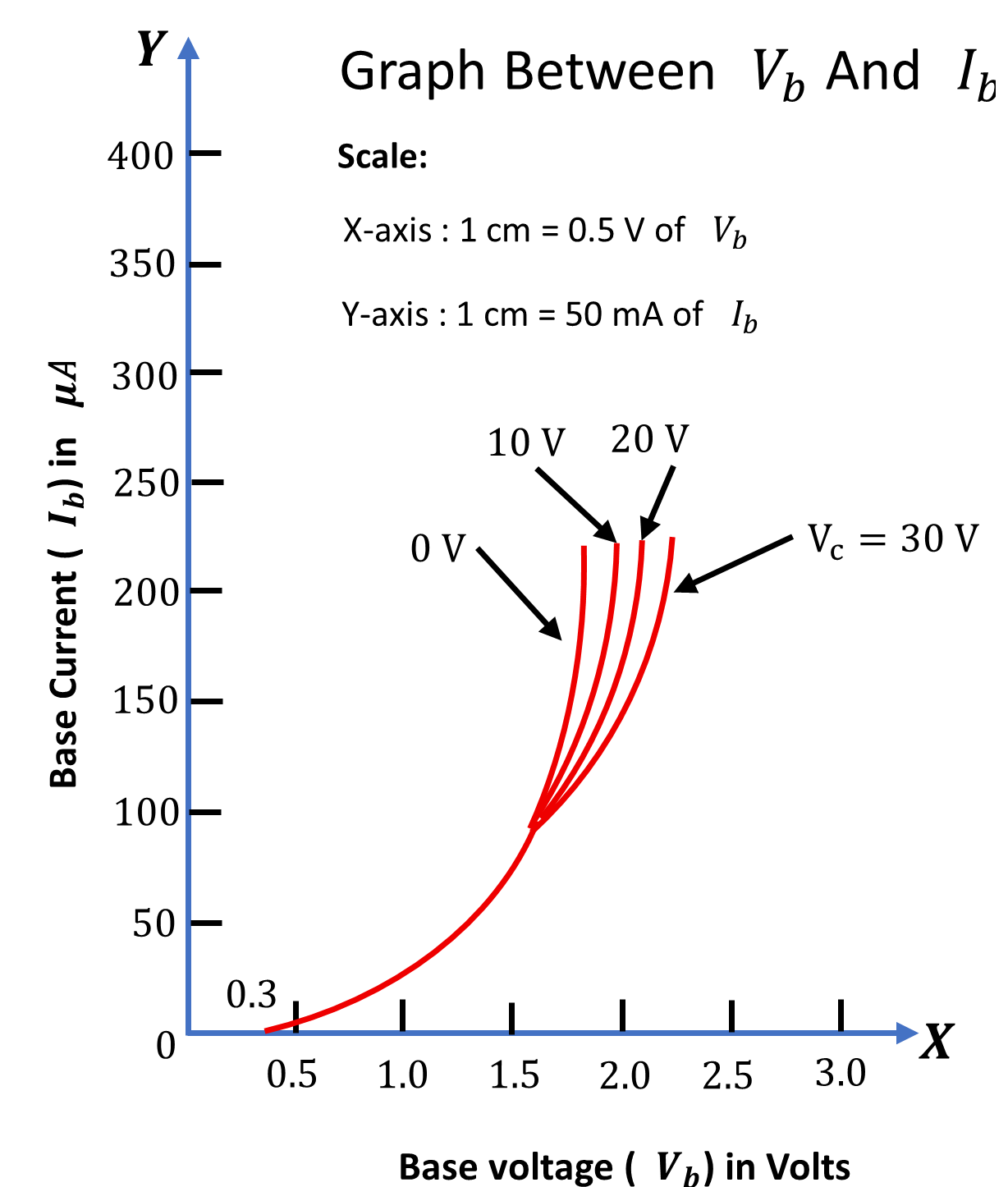
Plot a graph between base voltage Vb and base current lb for zero collector voltage Vc, taking Vb along X-axis and lb along Y-axis. Plot graphs for different values of Vc. The graphs come as shown. These graphs are called 'input characteristics' of the transistor.
The slope of graphs becomes large at the ends. The slope gives value of $\frac{\Delta I_b}{\Delta V_b}$. Its reciprocal $\frac{\Delta V_b}{\Delta I_b}$ gives input resistance $\mathrm{R}_{\mathrm{I}}$. As graphs run parallel near the ends, all give same value of $R_1$.
![]()
2. Calculation for output resistance $\left(\mathrm{R}_0\right)$
Plot a graph between collector voltage $\mathrm{V}_{\mathrm{c}}$ and collector current $\mathrm{I}_{\mathrm{c}}$ for $10 \mu \mathrm{~A}$ base current $\mathrm{l}_{\mathrm{b}}$, taking $\mathrm{V}_{\mathrm{c}}$ along X -axis and $I_{\mathrm{c}}$ along Y -axis. Plot graphs for different values of $\mathrm{l}_{\mathrm{b}}$.
![]()

These graphs are called 'output characteristics' of the transistor.
near the ends, all give same values of $R_0$.
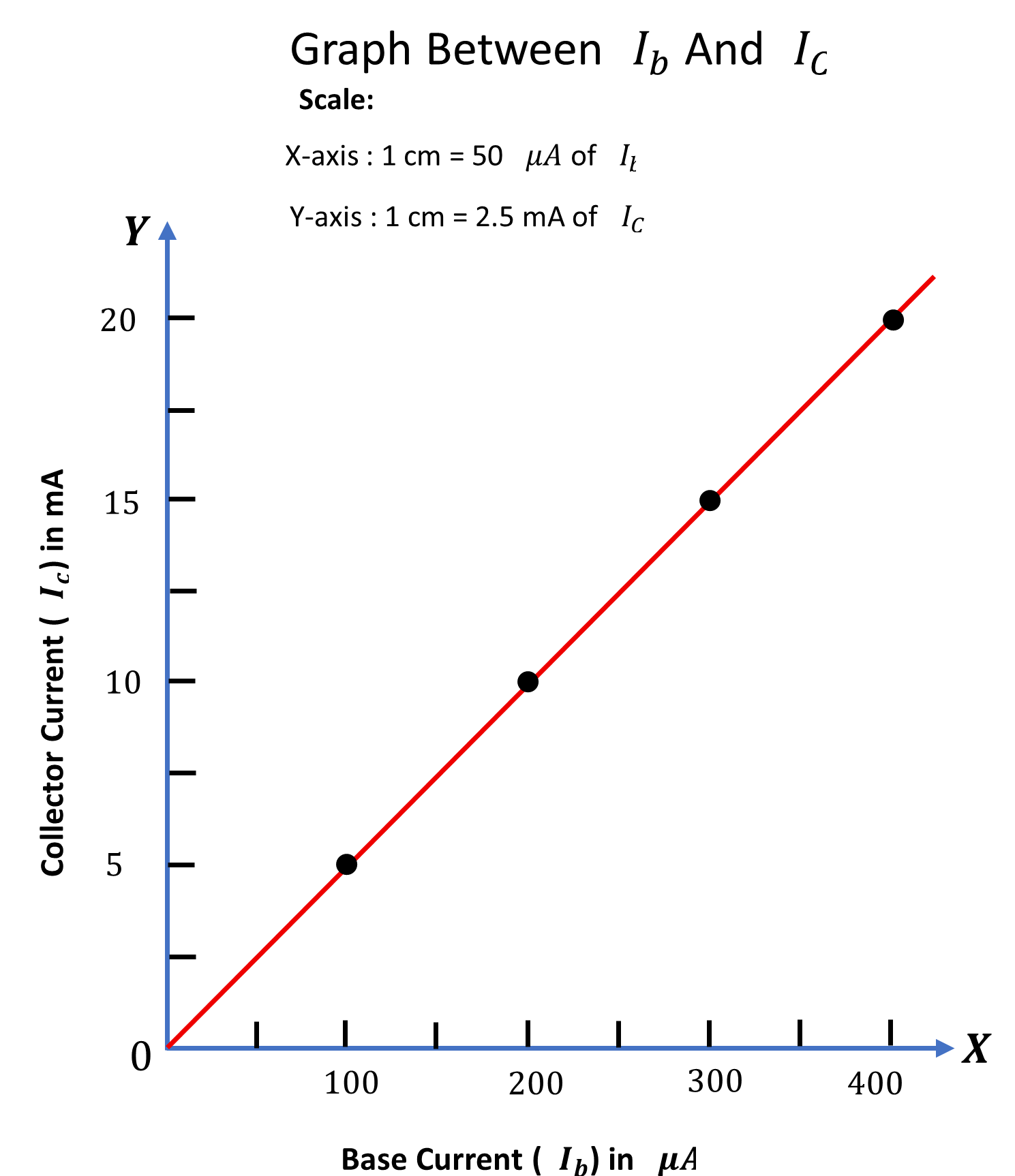
3. Calculation for current gain $(\beta)$
Plot a graph between base current $\mathrm{I}_{\mathrm{b}}$ ) and corresponding collector current $\mathrm{I}_{\mathrm{c}}$ ( for 30 volts collector voltage ) $\mathrm{V}_{\mathrm{c}}, \mathrm{t}$ along Y -axis. The graph comes to be a straight line. The graph is called current gain characteristic of the common
The slope of the straight line gives value of $\frac{\Delta I_c}{\Delta I_b}$ which is the value of current gain $\beta$ of the common emitter transistor
![]()
4. Calculation for voltage gain $A_v$
From relation, Voltage gain $=$ Current gain $\times$ Resistance gain
$
A_v=\beta \times \frac{R_0}{R_I}
$
Result
For the given common emitter transistor,
Current gain, $\beta=\ldots$.
Voltage gain, $\quad A_v=\ldots \ldots$
"Stay in the loop. Receive exam news, study resources, and expert advice!"
Get Answer to all your questions
B.Tech/B.Arch Admissions OPEN
Among top 100 Universities Globally in the Times Higher Education (THE) Interdisciplinary Science Rankings 2026
UPES B.Tech Admissions 2026
ApplyLast Date to Apply Extended till Today, 30th April | Ranked #43 among Engineering colleges in India by NIRF | Highest Package 1.3 CR , 100% Placements
Amrita University B.Tech 2026
ApplyRecognized as Institute of Eminence by Govt. of India | NAAC ‘A++’ Grade | Upto 75% Scholarships
MAHE, Manipal - B.Tech Admissions 2026
ApplyExtended Application Deadline: 30th April | NAAC A++ Accredited | NIRF Rank #3
Reva University B.Tech Admissions 2026
ApplyQS I-Gauge Diamond Rated | NAAC A+ Accredited | 621 Recruitment Partners | INR 40 LPA Highest CTC | 4482 Job offers
Manav Rachna-B.Tech Admissions 2026
ApplyNAAC A++ Grade | Recognized as Category-1 Deemed to be University by UGC | 41,000 + Alumni Imprints Globally